


Why Orbital Semiconductors Matter
The semiconductor industry is reaching a bottleneck: terrestrial fabs are constrained by land, energy, and contamination control. Even the most advanced cleanrooms cannot fully eliminate particulate matter, a critical factor for the next generation of power‑management chips. Besxar’s approach flips the paradigm by moving the fabrication process into the vacuum of space, where the absence of atmosphere and the ability to isolate wafers from terrestrial contaminants can dramatically improve yield and purity.
Key benefits include:
- Ultra‑clean environment: Space offers a particulate‑free vacuum, reducing defect rates.
- Thermal stability: Orbital temperature cycles can be precisely controlled for deposition processes.
- Rapid iteration: Each Falcon 9 flight can deliver a new batch of wafers, accelerating R&D cycles.
These advantages align with the growing demand for high‑performance chips in data centers, electric vehicles, and robotics—markets that require tighter control over power efficiency and reliability.
Besxar’s Technology Stack
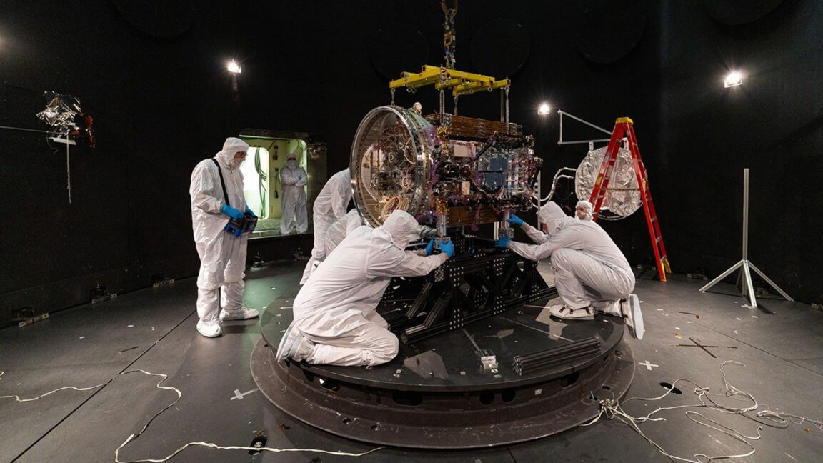
Besxar’s orbital fabrication strategy is built around a modular payload called a fabship. The first two canisters were flown on a July Starlink mission, proving the concept of launching semiconductor precursors and returning them for analysis.
Fabship Design
- Canister architecture: Lightweight, hermetically sealed containers that protect wafers during launch and exposure to space vacuum.
- Thermal control: Passive radiators and active heaters maintain deposition temperatures.
- Data telemetry: Onboard sensors record temperature, pressure, and particulate levels for post‑flight analysis.
The July flight demonstrated that the canisters survived launch stresses and that returned wafers exhibited the cleanest particulate profiles compared to terrestrial counterparts. A malfunction in the flight data system of one canister is currently under investigation, underscoring the iterative nature of this pioneering effort.
Planned Upgrades
Over the next two years, Besxar plans iterative upgrades to increase wafer capacity and integrate additional deposition steps:
- Heating wafers to the required temperatures for material synthesis.
- Depositing a single material layer to form the initial semiconductor structure.
- Sequentially adding layers to build complex multi‑layer devices.
These steps mirror conventional fab processes but are adapted for the constraints of orbital payloads.
Flight Program and Milestones
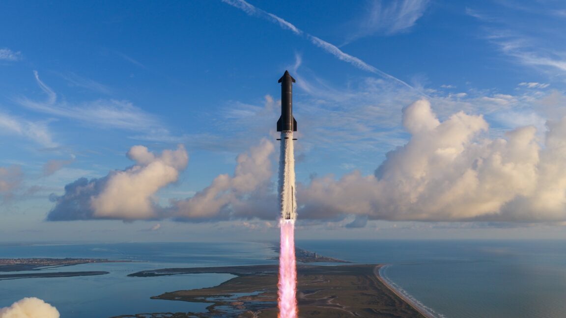
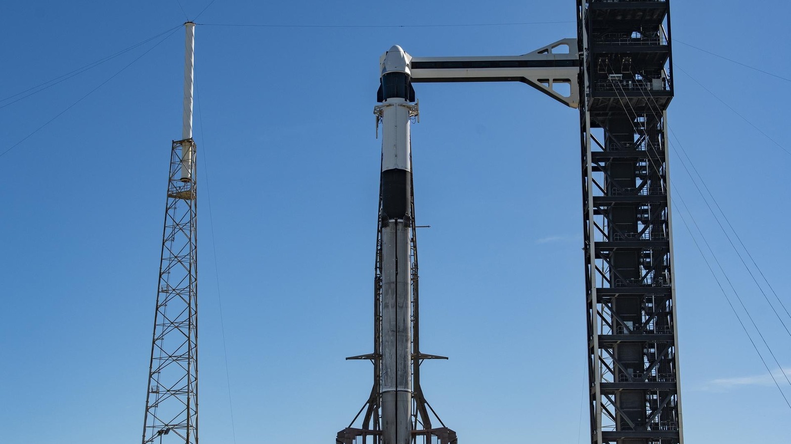
Besxar’s current strategy leverages SpaceX’s Falcon 9 boosters, which have completed 163 round‑trips last year and more than 100 this year. The company intends to prototype an orbital semiconductor factory across a dozen flights.
| Milestone | Description | Status |
|---|---|---|
| First two fabships | Demonstrated launch survival and wafer cleanliness | Completed (July Starlink) |
| Future fabships | Incremental capacity and process steps | Planned (next 2 years) |
| Large orbital fab | Full‑scale fab aboard Starship | Long‑term goal |
The timeline reflects a cautious approach: by de‑risking technology on Falcon 9, Besxar can validate processes before committing to Starship, which will enable larger payloads and higher wafer throughput.
Competitive Landscape
Besxar is not alone in exploring space
Besxar is not alone in exploring space‑based semiconductor production. United Semiconductors announced a partnership with a European launch provider to test a “micro‑gravity deposition chamber” on a Vega‑C flight, while Space Forge is field‑testing a 3‑U CubeSat that performs atomic‑layer deposition (ALD) on silicon wafers. Both firms are targeting similar high‑purity power‑management chips, but their approaches differ: United Semiconductors plans to use a single‑use chamber that is discarded after each flight, whereas Space Forge is developing a reusable orbital platform that will dock with a future lunar gateway.
Potential future competitors include Rocket Lab and Stoke Space, which are racing to field next‑generation reusable launch vehicles capable of delivering larger payloads at lower cost than Falcon 9. If they succeed, the economics of orbital fabs could shift dramatically, opening the door for even more ambitious production volumes.
Funding & Investor Landscape
Besxar’s capital raise reflects growing investor confidence in the “space‑fab” thesis:
| Funding Round | Amount | Lead Investors | Notable Participants |
|---|---|---|---|
| Seed (2025) | $9 M | Dauntless Ventures, Overture VC | Space Capital, Lux Capital |
| Bridge (2026) | $4.5 M | Dauntless Ventures (follow‑on) | Andreessen Horowitz (strategic) |
| Total | ~$13.5 M | — | — |
The bridge round, closed in March 2026, is earmarked for the next three fabship iterations and for scaling the data‑telemetry pipeline that will feed machine‑learning models used to optimize deposition parameters in orbit.
Market Opportunity
The target market for Besxar’s ultra‑clean wafers is the high‑efficiency power‑management segment of the semiconductor industry. According to IDC, global demand for power‑ICs in data‑center servers, electric‑vehicle power‑train controllers, and industrial robotics is projected to grow at a CAGR of 12 % through 2035, reaching $18 B in annual revenue. Even a modest 0.5 % market share for space‑fabricated wafers would translate to $90 M in sales per year, well above the current R&D spend of most fab‑as‑a‑service startups.
Technical Challenges & Risk Mitigation
| Challenge | Description | Mitigation Strategy |
|---|---|---|
| Radiation‑induced defects | High‑energy particles can create lattice damage in silicon. | Use radiation‑hardening shielding and schedule flights during solar minimum periods. |
| Thermal cycling stress | Repeated heating/cooling can cause wafer warping. | Implement active thermal control loops and conduct extensive ground‑based thermal‑vacuum testing. |
| Data latency | Telemetry bandwidth limits real‑time process monitoring. | Store high‑resolution sensor data onboard and downlink after each orbit; employ edge‑AI for on‑board anomaly detection. |
| Regulatory compliance | Export controls on advanced semiconductor tech. | Work with the Department of Commerce to secure EAR licenses; keep critical IP on Earth‑based ground stations. |
Besxar’s engineering team is already integrating radiation‑tolerant CMOS sensors and developing a “digital twin” of each fabship that runs in parallel on Earth, allowing rapid post‑flight analysis and iterative design improvements.
Timeline & Future Flights
| Quarter | Milestone | Expected Outcome |
|---|---|---|
| Q4 2026 | Fabship 3 launch on Falcon 9 (capacity ↑ 2×) | Demonstrate two‑step deposition (substrate heating + first material layer). |
| Q2 2027 | Fabship 4 with in‑orbit diagnostics | Validate real‑time thickness monitoring via spectroscopic ellipsometry. |
| Q4 2027 | Pilot batch of 50 wafers returned | Achieve >99.9 % defect‑free yield, ready for limited‑scale customer trials. |
| 2028‑2029 | Starship‑compatible fabship prototype | Scale payload to 200 kg, enabling multi‑hundred wafer runs per flight. |
| 2030+ | Full‑scale orbital fab (≥10 m³) aboard Starship | Target production of 10,000 wafers per launch, entering commercial supply contracts. |
The roadmap deliberately staggers hardware upgrades with incremental funding rounds, ensuring that each flight de‑risks the next.
Outlook & Industry Impact
If Besxar’s incremental approach succeeds, the semiconductor supply chain could gain a new “clean‑room in the sky” that complements terrestrial fabs. The ability to iterate quickly—flipping a new fabship into orbit within weeks—offers a level of agility unheard of in the multi‑year cycle of traditional fab upgrades. Moreover, the technology could eventually be repurposed for other high‑purity materials, such as quantum‑dot arrays or advanced photonic crystals, broadening the commercial addressable market.
However, the path is not without hurdles. The economics hinge on sustained low launch costs, which remain tied to SpaceX’s ability to reuse Falcon 9 boosters at scale and, later, to Starship’s operational cadence. Additionally, the industry will watch closely how regulatory bodies treat the export of space‑fabricated semiconductor IP.
Conclusion
Besxar’s modest but methodical program—starting with two proof‑of‑concept fabships and scaling toward a Starship‑borne orbital fab—illustrates a pragmatic route to commercializing space‑based chip manufacturing. By leveraging the vacuum of orbit, the startup aims to deliver wafers with unprecedented purity, targeting the power‑efficiency demands of tomorrow’s data centers, EVs, and robots. As launch costs continue to fall and competitors race to stake their own claims in the microgravity fab arena, the next few years will determine whether orbital semiconductor production moves from a scientific curiosity to a viable component of the global chip supply chain.
Frequently Asked Questions
Q: How does a wafer survive launch stresses and re‑entry?
A: Fabships are built with a carbon‑fiber composite shell and internal shock‑absorbing mounts that decouple the wafer carrier from launch vibration. After the orbital experiment, the canister is sealed and placed in a heat‑shielded payload fairing for controlled re‑entry, where it lands under parachute for recovery.
Q: Why not simply improve cleanrooms on Earth?
A: Terrestrial cleanrooms still contend with airborne particles, outgassing, and limited thermal stability. Space offers a natural ultra‑high vacuum and eliminates many sources of contamination, enabling defect rates that are difficult to achieve on the ground.
Q: When will customers be able to purchase space‑fabricated wafers?
A: Besxar plans to begin limited‑scale commercial shipments after the pilot batch in late 2027, pending successful qualification of the fabship process and completion of required export‑control licensing.
Q: Is the technology compatible with existing semiconductor manufacturing equipment?
A: Yes. The wafers returned from orbit are processed using standard backside‑polishing and packaging lines. Besxar’s value proposition lies in the upstream material purity; downstream steps remain unchanged.
Q: Could this approach be used for other materials beyond silicon?
A: The modular fabship architecture is material‑agnostic. Besxar is already investigating deposition of gallium nitride (GaN) and silicon‑carbide (SiC) layers, which could benefit high‑power RF and power‑electronics markets.
Source: Original Article