







Why AI Is a Game‑Changer for Modern Fab Operations
The semiconductor road‑to‑market has always been a race against physics. As transistor dimensions shrink below 5 nm, the number of process steps climbs, and the tolerance window narrows to a few nanometers. A single mis‑aligned exposure or an unexpected defect can cost millions of dollars in lost yield. Traditional trial‑and‑error on the production line is no longer viable; each experiment consumes precious silicon, time, and capital.
Artificial intelligence intervenes at three critical junctures:
- Predictive Modeling – Physics‑informed neural networks learn the underlying equations of plasma chemistry, diffusion, and stress, delivering accurate forecasts without a full finite‑element run.
- Accelerated Computing – GPU‑optimized libraries such as NVIDIA cuDSS and cuLitho compress multiphysics workloads by an order of magnitude, turning hour‑long simulations into minutes.
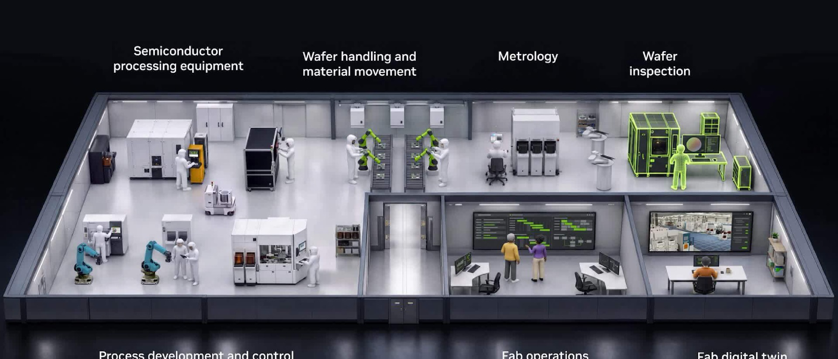
- Digital Twins – End‑to‑end virtual replicas of the fab allow engineers to “run” a wafer through every step before any wafer ever leaves the cleanroom.
Together, these capabilities form an AI‑defined fab where engineers spend less time waiting for answers and more time exploring alternatives. The shift mirrors broader AI adoption trends discussed in articles like Reverse Game Theory: Guiding Super‑Intelligent AI, highlighting how intelligent agents can augment, rather than replace, human expertise.
Industry Impact: Faster Time‑to‑Market and Higher Yields
Shortening the Design‑to‑Production Loop
Historically, a new node required 12–18 months of iterative lithography, etch, and deposition experiments. With AI‑driven acceleration:
- Multiphysics simulations (heat, electrical, mechanical) run up to 10× faster using COMSOL’s cuDSS integration. Engineers can evaluate dozens of equipment‑parameter combos in a single day.
- Atomic‑scale discovery platforms like Applied Materials’ Ginestra, powered by NVIDIA Physics Ne Mo, achieve 35× speed‑ups for topography predictions, enabling rapid material screening.
- Computational lithography benefits from Siemens’ cuLitho integration, delivering up to 17× acceleration on critical mask‑optimization workloads.
The net effect is a reduction of the prototype cycle from weeks to hours, allowing manufacturers to lock in process windows before silicon is even processed.
Yield Improvement and Cost Reduction
Yield loss is the single biggest cost driver in high‑volume manufacturing. AI contributes in three ways:
- Root‑Cause Attribution – AI agents correlate defect maps with process parameters, pinpointing the most probable cause within minutes.
- Predictive Yield Models – Trained on historical fab data, these models forecast wafer‑level yield for a given recipe, flagging low‑yield scenarios before they materialize.
- Dynamic Process Control – Real‑time inference adjusts gas flows, temperature setpoints, and exposure doses on the fly, maintaining optimal conditions throughout the run.
A conservative industry study estimates 5–7 % yield uplift for nodes 3 nm and below when AI‑assisted control is deployed, translating into billions of dollars of additional revenue for leading foundries.
Technical Breakdown: How the AI Stack Is Built
1. Physics‑Based Neural Networks
Unlike black‑box models, physics‑informed networks embed conservation laws directly into their architecture. For plasma etch, the network learns the coupled Poisson–Nernst–Planck equations governing ion transport, while respecting charge neutrality. Training data comes from a curated set of high‑fidelity CFD simulations and select in‑fab measurements. Once trained, the model can predict ion density profiles for new gas mixtures in milliseconds.
2. GPU‑Optimized Simulation Libraries
The NVIDIA cuDSS (CUDA Deep Simulation Suite) library provides GPU kernels for:
- Finite‑difference time‑domain (FDTD) electromagnetic solvers used in lithography.
- Coupled thermal‑mechanical solvers for stress analysis in 3‑D stacked dies.
- Monte‑Carlo particle transport for radiation‑hardening studies.
By offloading these kernels to modern Ampere‑based GPUs, compute throughput scales linearly with the number of GPUs, enabling cluster‑wide acceleration without rewriting legacy Fortran code.
3. Digital Twin Architecture
A digital twin consists of three layers:
| Layer | Function | Example Tool |
|---|---|---|
| Data Ingestion | Real‑time sensor streams (temperature, pressure, metrology) | Kafka + NVIDIA RAPIDS |
| Model Execution | Runs physics‑based AI models and accelerated simulations | cuDSS, cuLitho |
| Decision Engine | Generates actionable recommendations for fab operators | Reinforcement‑learning agents |
The twin is continuously synchronized with the physical fab, ensuring that any deviation is instantly reflected in the virtual environment.
4. AI Agents for Workflow Automation
Complex engineering tasks—such as “run a plasma simulation, compare with metrology, and adjust gas flow”—are now orchestrated by autonomous agents. These agents:
- Parse engineering intent from natural‑language tickets.
- Select the appropriate model (full simulation vs. surrogate).
- Execute the job on the GPU cluster and log results.
- Notify the engineer with a concise decision summary.
The result is a 10–20× reduction in manual coordination effort, freeing senior engineers to focus on strategic innovation.
Future Outlook: From AI‑Defined to AI‑Autonomous Fabs
The current generation of AI tools is assistive: engineers retain final authority, while AI supplies rapid insights. The next frontier is AI‑autonomous fabs, where closed‑loop control systems make real‑time adjustments without human intervention. Key enablers include:
- Edge AI – Deploying inference models directly on equipment controllers to eliminate network latency.
- Federated Learning – Sharing model updates across multiple foundries while preserving proprietary data, accelerating collective knowledge growth.
- Explainable AI (XAI) – Providing transparent reasoning for each control decision, essential for regulatory compliance and trust.
As these technologies mature, the semiconductor ecosystem will likely see continuous process optimization, where each wafer contributes to a self‑improving model that drives the next wafer’s parameters. This vision aligns with broader AI governance discussions, such as those explored in Trump’s ‘Super Intelligence’ Rebrand: Politics Meets AI, emphasizing the need for responsible AI deployment.
Frequently Asked Questions
Q1: Do AI‑accelerated simulations replace physical experiments entirely? A: No. They dramatically reduce the number of required experiments by filtering out low‑probability candidates, but final validation on silicon remains essential for qualification.
**Q2: How much hardware investment is needed
repeated full‑physics runs for every recipe tweak. By training a physics‑informed neural network on a curated dataset of high‑fidelity plasma simulations, engineers can obtain near‑real‑time predictions of ion density, radical concentration, and surface temperature for new gas mixtures or power settings. The surrogate model runs on a single GPU in under a second, compared to the several minutes or hours required for a conventional CFD solve. This capability enables a design‑of‑experiments loop that explores dozens of process windows in the time it used to take to evaluate one.
AI‑Driven Root‑Cause Analysis and Defect Attribution
When a defect pattern appears on a wafer, the traditional workflow involves manual correlation of metrology data, process logs, and equipment histories—a process that can take days. Modern AI agents automate this pipeline:
- Data Fusion – Using NVIDIA RAPIDS, terabytes of sensor streams, inspection images, and recipe logs are merged into a unified feature matrix.
- Anomaly Detection – Unsupervised models such as variational autoencoders flag outlier runs that deviate from the statistical norm.
- Causal Inference – Graph‑based Bayesian networks evaluate the probability that each process step contributed to the observed defect, ranking the most likely culprits.
The result is a root‑cause hypothesis delivered to the engineer within minutes, allowing rapid corrective action and minimizing yield loss.
Digital Twin in Action: A End‑to‑End Wafer Flow
Consider a 7 nm logic wafer moving through a typical fab line:
- Pre‑process Simulation – The digital twin predicts film thickness uniformity after deposition using the accelerated COMSOL‑cuDSS model.
- Lithography Optimization – Siemens’ cuLitho evaluates mask‑error‑enhancement‑factor (MEEF) across the entire field, suggesting exposure dose adjustments that reduce line‑edge roughness.
- Etch Forecast – The plasma surrogate model estimates sidewall profile evolution for the proposed etch chemistry, flagging potential micro‑loading issues.
- Metrology Feedback – In‑line scatterometry data is fed back into the twin, updating the Bayesian process model in real time.
- Decision Engine – A reinforcement‑learning agent proposes the optimal recipe tweak that maximizes projected yield while staying within equipment constraints.
Because the twin mirrors the physical fab, the engineer can “run” the wafer virtually, observe the downstream impact of each decision, and approve the best‑performing recipe before any silicon touches the line.
Scaling AI Across the Fab: Infrastructure Considerations
Deploying the AI stack at fab scale demands a robust compute and data pipeline:
| Component | Recommended Specification | Role |
|---|---|---|
| GPU Cluster | 8× NVIDIA H100 GPUs per node, NVLink interconnect | Accelerated simulations, surrogate inference |
| Data Lake | Object storage (e.g., Amazon S3 or on‑prem Ceph) with RAPIDS‑compatible parquet files | Long‑term sensor and metrology archive |
| Orchestration | Kubernetes with NVIDIA GPU Operator | Job scheduling, auto‑scaling of workloads |
| Security | Zero‑trust networking, role‑based access control (RBAC) | Protect IP and production data |
By containerizing each AI service (simulation, surrogate, decision engine), fabs can achieve continuous integration/continuous deployment (CI/CD) for model updates, ensuring that the latest physics insights are always available to engineers.
From Assistive to Autonomous: The Road Ahead
While today’s AI‑defined fab still relies on human validation, several emerging trends point toward AI‑autonomous fabs:
- Edge‑Embedded Inference – Deploying lightweight models directly on equipment controllers enables sub‑millisecond feedback loops for gas flow or laser power adjustments.
- Federated Model Training – Multiple foundries can collaboratively improve plasma and lithography models without sharing raw data, preserving competitive advantage while accelerating learning.
- Explainable AI (XAI) – Techniques such as SHAP values and counterfactual analysis provide transparent rationales for each control decision, satisfying both engineers and regulatory auditors.
When these capabilities mature, the fab will continuously self‑optimize: each wafer’s data refines the twin, the twin proposes the next recipe, and the edge controller implements it—all without manual intervention unless a confidence threshold is breached.
Conclusion
AI is no longer a peripheral add‑on for semiconductor manufacturing; it is becoming the central nervous system of the modern fab. By coupling physics‑informed neural networks with GPU‑accelerated simulation libraries and high‑fidelity digital twins, engineers can:
- Explore far more process alternatives in a fraction of the time, shrinking design cycles from weeks to hours.
- Identify and remediate defects within minutes, protecting yield and reducing costly re‑runs.
- Maintain a living, data‑rich replica of the fab that informs every decision from material selection to final mask alignment.
The transition from AI‑assisted to AI‑autonomous fabs promises even greater efficiencies, but it also underscores the need for responsible AI governance, explainability, and robust infrastructure. As the industry embraces these tools, the pace of innovation will accelerate, enabling the next generation of chips that power everything from AI‑driven edge devices to quantum‑ready processors.
Frequently Asked Questions (Extended)
Q3: How do physics‑informed neural networks differ from traditional machine‑learning models? Answer: They embed governing equations (e.g., Maxwell’s equations, Navier‑Stokes) directly into the loss function, ensuring that predictions obey physical laws even when extrapolating beyond the training data. This reduces the amount of labeled data required and improves trustworthiness.
Q4: What is the typical latency for a surrogate plasma model in production? Answer: On an NVIDIA H100 GPU, inference for a full 3‑D plasma profile completes in ≈0.8 seconds, compared to 5–10 minutes for a full CFD solve on a CPU cluster.
Q5: Can existing legacy simulation code be accelerated without a full rewrite? Answer: Yes. NVIDIA’s cuDSS provides GPU‑offload wrappers for common finite‑difference and finite‑element kernels, allowing legacy Fortran or C++ codebases to call GPU‑accelerated routines with minimal code changes.
Q6: How is data security handled when using federated learning across multiple fabs? Answer: Model updates are exchanged as encrypted weight deltas, never raw sensor data. Each participant trains locally on proprietary data, then aggregates updates via a secure aggregation protocol, ensuring IP remains confidential.
Q7: What skill set do engineers need to work effectively in an AI‑defined fab? Answer: A blend of domain expertise (process physics, lithography, etch chemistry) and data‑science fluency (Python, GPU programming, model interpretability). Many fabs are establishing “AI‑process engineer” roles that bridge these disciplines.
Q8: Will AI replace human engineers in the fab? Answer: No. AI augments human expertise by handling repetitive, data‑intensive tasks and providing rapid insights. Human engineers remain essential for hypothesis generation, strategic decision‑making, and overseeing AI governance.
Embracing AI today positions semiconductor manufacturers to meet the relentless demand for smaller, faster, and more efficient chips—while keeping yields high and costs low.
Source: Original Article